Pressure Sensor & Interface: Technical
By David Clarke [21030085++] <ac151@ncf.ca>How Does It Work?
Basic Theory of Operations
By default the Chroma accepts analog control voltages, converts them to digital signals, inputs them into the main computer and manipulates them accordingly.
This general signal flow is seen in the operation of the performance levers to the left of the keyboard and the volume pedal.
Both of these items vary a voltage that is then used by the computer to manipulate other voice parameters.
In terms of implementation, the Chroma uses an Analog to Digital Converter (ADC). The ADC converts all of the external analog voltages into digital signals that can be manipulated/acted upon by the main microprocessor.
During the design of the Chroma, one input to the ADC was reserved for pressure information.
At a conceptual level, if keyboard pressure could somehow be converted into a variable voltage (as is done for the performance levers or the volume pedal), then such a 'pressure voltage' could be handled in a similar way - fed into the ADC and used for whatever purposes the firmware might like.
The ADC is configured to convert input voltages between 0v and 5v, 0v representing a digital 0 output and 5v representing digital full-scale, or 0xFF.
To implement a pressure sensor interface then, it is necessary to convert key pressure into a voltage signal between 0 and 5v.
Pressure Sensor Implementation
Overview
While it is conceptually simple to say an interface should convert pressure into a voltage between 0 and 5v, the physical implementation is somewhat involved.
First, since the pressure response is to be polyphonic, there has to be a method to read pressure on a key-by-key basis. This means that each key has to have its own 'sensor.' It also means that while one sensor is being read, the other ones should not interfere.
The second difficulty of implementation is that the specific voltage from the sensors will likely not be exactly in the form expected by the ADC. That means there will have to be some sort of scaling electronics to ensure that the range of 'no pressure' to 'full pressure' will span the full range of the ADC input (0 to 5v). This same electronics will have to also compensate for any non-linearities in the pressure response.
As implemented in the Chroma, the Pressure Sensor consists of key sensors and signal conditioning electronics. The following sections provide details on their implementation.
(Note: The Chroma has 64 keys. Depending on the point of reference, they might be referred to as Key #'s 1-64 or 0-63. Where possible the former convention is used in this document).
Electronic Detail
Key Sensors
Figure 8 is a pictorial representation of the individual key sensors in the Chroma. Each key's sensor behaves as a variable resistance, with infinite resistance at 'no pressure.'
By selecting one column (KEY_A through KEY_H) and one row (BANK1 through BANK8), a single 'variable resistor' sensor associated with a key can be selected.
Key Selection
Figure 9 identifies the electronics used to select the individual keys.
Z2 (a 1-of-10 decoder/driver) uses signals KS2 - KS0 to select one of 8 outputs. These outputs are pulled up to 5V (through resistor pack Z1) when not selected - and are driven low when selected. The three binary bits of KS2 - KS0 select one of eight columns (KEY_A through KEY_H).
With reference to Figure 8, if a given KEY column is driven low, that will connect 8 different keys low (e.g., if KEY_A is driven low then K1, K9, K17, K25, K33, K41, K49 and K57 are all connected to ground, at one end).
Z3 (an 8-Channel Analog Multiplexer/Demultiplexer) accepts the 8 separate row inputs (BANK1 - BANK8). It then uses KS5 - KS3 to select just one of these outputs.
With this arrangement, the 6 key select bits (KS5 - KS0) can select the pressure sensor for a single key, connect one side of it to ground, and allow the other side to be routed to the output of Z3 (pin 3).
(Note: The while the Rhodes Pressure Sensor circuit board does show the reference designators for the integrated circuits, Z1 - Z5, it does not provide references for the individual resistors or capacitors. In order to be able to discuss the use of these components, Figure 10 was generated to provide a correlation between the physical location of a component and what they are called in this document).
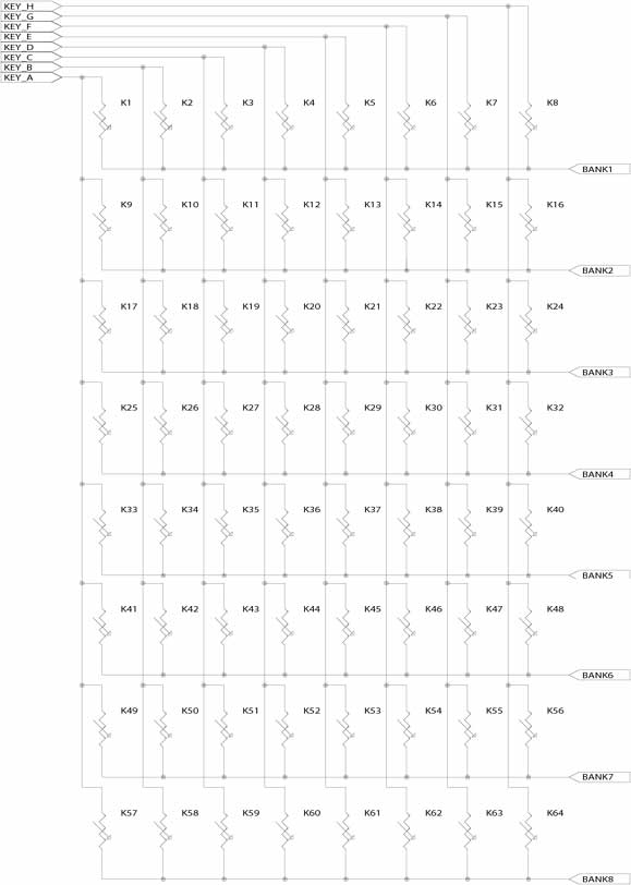
Figure 8: Key Sensor Matrix (PDF Version, 64K)
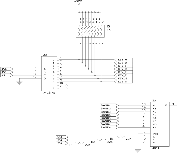
Figure 9: Row/Column Selecting Circuitry
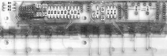
Figure 10: Reference Designation Assignment
Sensitivity Adjustment
If a fixed amount of pressure is asserted on keyboard 1, it should have the same affect if that same, fixed amount of pressure is asserted on keyboard 2. In practice, component variation and implementation specifics mean that there will be slight differences between how the pressure interface responds in one machine versus another.
To further complicate matters - the individual key pressure sensors are actually implemented on two separate circuit boards (connected by a flexible cable, as shown in Figure 4).
Due to expected variation in materials used, it is almost as if the Chroma has two pressure sensors installed in each keyboard.
In order to have a consistent feel across the keyboard, it is necessary to be able to compensate for difference between keyboards, and between the two sensor boards in a single keyboard.
The Chroma designers did include such an adjustment capability on the Chroma pressure sensor.
As noted earlier, KS5 - KS0 will uniquely select one of 64 keys. As implemented, the number of the key selected corresponds directly to the binary number resulting from the 6 bits of KS5 to KS0.
By way of example we would have:
| KS5 | KS4 | KS3 | KS2 | KS1 | KS0 | Key Selected Is: |
|---|---|---|---|---|---|---|
| 0 | 0 | 0 | 0 | 0 | 0 | Key 1 |
| 0 | 1 | 1 | 1 | 1 | 1 | Key 32 |
| 1 | 0 | 0 | 0 | 0 | 0 | Key 33 |
| 1 | 1 | 1 | 1 | 1 | 1 | Key 64 |
Based on this relationship, we can see that when KS5 = 0, any of the lower 32 keys on the keyboard can be accessed. When KS5 = 1, the upper 32 keys can be accessed. Since the two pressure sensor boards each span half of the keys (32), the KS5 signal can be used to indicate which pressure sensor board is currently being accessed (the left one, with keys 1-32 or the right one with keys 33-64).
Using this relationship, individual compensation can be applied to the two different boards as shown in Figure 11.
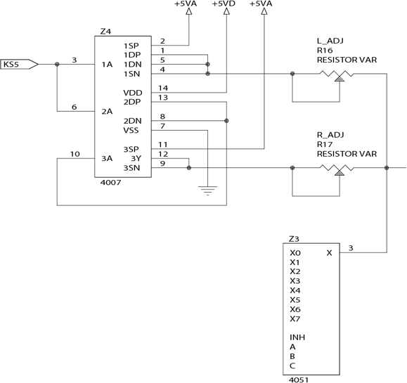
Figure 11: Pressure Scaling Adjustment
Z4 contains three N-channel/P-channel MOS transistor pairs.
When KS5 = 0 the P-channel transistor in pair #1 conducts, connecting analog +5V to R16. In a similar way, when KS5 = 0, the P-channel transistor in pair #2 also conducts, connecting the common point (2DP/2DN) to +5V digital. This output goes as an input to pair #3. The high signal causes the P-channel transistor in pair #3 to be non-conducting, effectively disconnecting R17.
When KS5 = 1, the operation noted above is essentially reversed, and R16 will be disconnected, with R17 being connected to analog +5V.
So, depending on the state of KS5, either R16 or R17 will be connected to +5V at one end, and to the output of Z3 at the other end. In this way, R16 and R17 can provide scaling to the pressure signal available at Z3, pin 3 - one resistor for each portion of the pressure sensor.
Signal Conditioning
In a simplified view of the configuration noted above, the pressure will appear as a variable resistance to ground connected to +5V via a scaling resistance, as depicted in Figure 12.
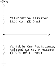
Figure 12: Simplified Raw Pressure Signal
When there is no pressure asserted, the variable key resistance is infinite. That would then mean that the output voltage (point A) is 5V.
When full pressure is asserted, the resistance doesn't go to zero, rather it is a finite value, and the voltage at point A generally drops to 3v.
So, the basic circuit would produce 5V at no pressure and 3v at maximum pressure. It is desired that the circuit produce 0v at no pressure and 5v at maximum pressure (to utilize the full range of the ADC, as well as to be in-line with how the other ADC inputs behave).
The output value needs to be conditioned. This is accomplished via the circuit in Figure 13.
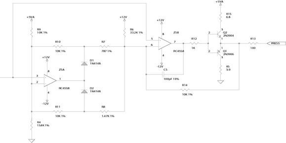
Figure 13: Signal Conditioning Electronics
The signal at the point labeled PRESS will have the characteristics mentioned earlier. Namely, it will be 0v when there is no pressure asserted for the specific key - and can go up to 5V for maximum pressure.
A complete, consolidated schematic is available in PDF format: PressureConsolidatedSchematic.pdf (72K).
Pressure Membrane
Figure 7 pictured the membrane which is 'pressed upon' to generate the pressure response. What is not clear in that figure is exactly how it pressure manages to get translated into a variable resistance.
Whereas on the default damper bar, the key strikes a thick piece of felt, the damper interface on the pressure sensor is much more complicated, being comprised of 6 separate layers (as shown below, in Figure 14).
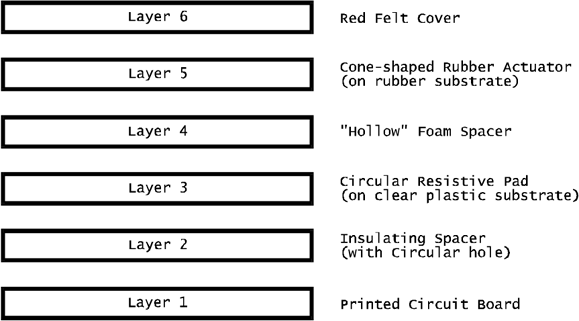
Figure 14: Stack-up of Pressure Membrane (Side-On View)
The following sections discuss the implementation of each of the 6 layers. For the sake of discussion, the diagrams will show the interface for a single key. (In practice there are actually 64 such areas on the pressure sensor.)
Layer 1 - PCB
On the printed circuit board itself (PCB), traces form an interdigital pattern - interwoven tracks that do not actually touch one another. With nothing to short the traces together, there is no connection from signal path A to signal path B, hence the interface behaves as an "open" under normal circumstances.
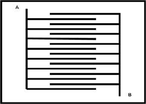
Figure 15: Interdigital Fingers on PCB
Layer 2 - Spacer with Hole
On top of the PCB is a relatively thin sheet of plastic, with a circular hole in the middle. This hole sits over the interdigital fingers on the PCB, as shown in Figure 16.
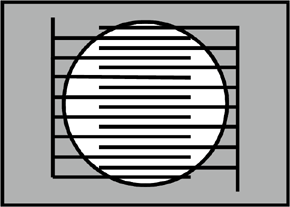
Figure 16: Spacer Overlaid on PCB
Layer 3 - Resistive Pad
The spacer discussed above is used to stand-off, or space away, a resistive element, so that when it sits in its natural position, it hovers over the traces. Figure 17 shows this pictorially.
The pad itself is a circular resistive area affixed to a plastic sheet.
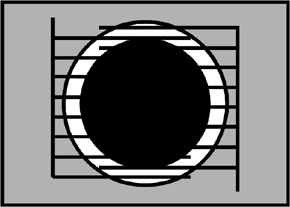
Figure 17: Resistive Pad
Layer 4 - Foam Spacer
Surrounding the resistive pad is a thick layer of foam rubber. This layer is what provides the "squish" to the pressure interface. It also serves as a spacer between the resistive pad and the rubber actuator.
The foam layer roughly follows the greyed area in Figure 17.
Layer 5 and 6 - Rubber Actuator and Key Interface (Felt)
Sitting on top of the foam spacer is a full layer of rubber. Where the rubber goes over the hole in the foam (which corresponds to the location of the resistive pad), there is a short cone of rubber.
This cone is tapered, as shown in the side-on view of Figure 18.

Figure 18: Tapered Actuator (side-view)
Just above the rubber layer is a layer of felt, which provides the physical interface to the keys.
When a key is pressed, it hits the felt, which in turn causes the tapered rubber actuator to press down through the foam spacer (which was previously holding it away from the resistive pad).
When only a light amount of pressure is asserted, just the tip of the actuator presses the pad, and so only the middle portion of the pad is pressed on to the PCB traces. The small amount of resistive material creates a resistive bridge between the fingers - and in essence creates a resistor of a particular value.
When the key is pressed harder, the actuator presses down harder, causing more of the cone's surface to press against the resistive pad. This in turn causes more area of the resistive pad to make contact with the interdigital traces on the PCB. The increased area leads to decreased net resistance.
In this way, the pressure on the interface relates to a corresponding, variable resistance value - the more pressure, the more surface area connected, and the lower the resistance.
Chroma Integration
Electrical Interface
On all I/O boards, J22 is provided with the following interface signals:
| Pin # | Name |
|---|---|
| 1 | +12V (Analog) |
| 2 | +5V (Analog) |
| 3 | KS5 |
| 4 | KS3 |
| 5 | KS1 |
| 6 | PRESS |
| 7 | Ground (Digital) |
| 8 | -12V (Analog) |
| 9 | Ground (Analog) |
| 10 | KS0 |
| 11 | KS2 |
| 12 | KS4 |
| 13 | PRESS |
| 14 | +5V (Digital) |
All these signals (with the exception of "PRESS") are inputs to the pressure sensor interface.
KS5 - KS0 are generated by Z30 on the I/O board. They are 6 data pins latched when the !WR_PRSS I/O strobe is activated.
Both PRESS signals are combined on the I/O board and go to PRESS input on Z3 (ADC0809), the analog to digital converter on the I/O board (8-bit ADC).
As connected, the ADC0809 will take input values from 0 to 5v and produce an 8-bit output.
Firmware Interface
Raw Data
The keyboard scanning computer is responsible to read key presses (and the velocity of those key presses) but it is not responsible for key pressure. Key pressure is read directly by the main 6809 CPU in the Chroma.
Key pressure is not read all the time, and it is not read for all the keys.
Firmware only reads pressure for those keys which are currently 'playing.' That is to say, it will request (and read) the pressure data for those keys what have an active channel.
The firmware scans which keys are playing and then will request the pressure of a particular key by placing the key number (0-63) on the data bus and then issuing a write to address $200E.
This will cause the key number to go out on KS5 to KS0, with KS5 being the most significant bit.
Since up to 16 notes could be playing at any one time, a maximum of 16 pressure measurements have to made during each pressure read cycle.
Firmware reads an individual key's pressure in just over 1.024mS (it uses a 1.024mS timer for the ADC conversion, and then some other time will be spent in general software overhead).
The pressure data for 16 notes can be read in approximately 20mS, meaning that pressure information can be updated 50 times per second.
Software Manipulation
While the 8-bit pressure data could have been read (and used) directly by firmware, the raw digital value is further manipulated.
The 8-bit value read from the ADC is divided by 4 so that the original pressure value in a range of 0-255 becomes a pressure value of 0-63. 0-63 is the same range used by the pressure command from the Chroma Interface.
Next: Q&A

